PVD carrier
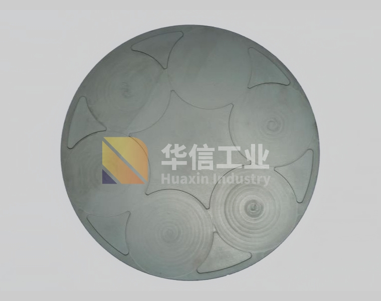
The silicon carbide PVD carrier plate was formed by isostatic pressing process and sintered at high temperature. According to the requirements of the user's design drawings, the outer diameter, thickness, the number and size of acupuncture points, the position and shape of the slot can be refined to meet the specific requirements of the user
- Typical application
- Features and advantages
- Specification
-
Typical application
PVD process in LED chip manufacturing, that is, physical vapor deposition.
-
Features and advantages
High density
Good thermal conductivity, low expansion coefficient and temperature equalization performance
Resistance to plasma impact
Resistant to various strong acid and alkali chemical reagents
After semiconductor grade cleaning -
Specification
Related Products


